64
Mega-Bytes of CPU Memory Storage.
16MB Pix.
Shows the first modification, 16MB.
64MB Pix.
Shows the second modification, 64MB.

I am looking for quads of these type of simms, just like these pictures
above.
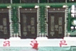
8 chips making 16MB on a single-sided 72-pin simm.
Or, 32MB using 16 of these chips on one 72-pin simm.
EDO or FastPage types, both work.
Remember this is only a theory,
and may not even work, but then it may, and that's why it is being pursued.
Here is another version of the NoCan series, a 32MB/64MB
interface. That's right, 32 or 64 Mega-Bytes. Let's see, that is
around 8 to 16 of the 4MB 30-pin type simms. Kinda overkill if you
ask me <really big grin here>. So far there is only 16MB installed,
to test this theory. Four each 4MB simms giving two banks of 8MB.
64MB was chosen only because the currently used CPLD ran
out of pins. A larger CPLD version could do up to 512MB, this would
use all 8 bits of the block $FF8x.
Oct 17, 2001 - 64MB board, is
now working. Am considering using 32MB simms, two each for the total.
There's now two setups, one 64MB and one 32MB.
Oct 3, 2001 - Working on a second
setup, a 64MB board, which is a modified/converted (read "butchered up")
2MB NoCan2 board.
Sept 20, 2001 - 72-pin simms
are now used. Made a 32MB plug-in. After fixing "several" wiring
errors, it booted RSDOS.
The simm type is 4MB x 32 bits,
8 chips per simm. These have the same DRAM chips that are on the
30-pin simms, ie 4mb x 4 bits, I think these are called 16MB simms. This
way 64mb will fit in four each 72 pin simm slots. This must be done
in pairs as the 72-pin simm -WR strobe is common to the whole simm.
Two simms are needed for a coco-3, -WE0 and -WE1. Each pair would
then give 32MB.
Sept 17, 2001 - It seems to
work and passes a machine code memory test.
A rommed "MTEST" has been implemented, and takes about
7 minutes to run and test most of all 16MB. It has been placed in
the disk 1.1 rom at $D8D0, since $D8D0 to $DEFF is unused.
At test end, test locations were examined and reported
$08, $4000. This means that all memory locations have been tested
from $01 through $07 in the sram, using memory from $4000 to $6000.
Sept 5, 2001 - Booted NitrOS-9
to make sure that the 2MB stuff stillworks, it does. Reports 1944
free, this is normal for my setup.
The 2MB interface
still exists and can be used as before, no changes there. The register
at $FF9B has only two bits there, for video. The bits at $FFA0-$FFAF,
D6 and D7 still go to the original SRAM and out to memory as before.
Here's what goes on. A block of SRAM (16
addresses by 8 bits) from $FF80 to $FF8F is write only. It is read
back by the system as $FFA0 to $FFAF. So, for each $FFAx memory block,
there's a corresponding $FF8x location to update.
For instance, let's
say that you want to use another block of the 32/64MB at $FFA2. You
do the appropriate 2MB setup, like before, then do the $FF82 setup additionally.
Order of writing to $FF8x or $FFAx is not important or required.
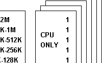
Has no video access, cpu memory only.
This is the one that is currently used, and being tested.
Anytime a $FFAx register is selected, the
corresponding $FF8x location must be used, ie. (x) nibbles must match.
for any access to $FFA0, use $FF80
for any access to $FFA1, use $FF81
for any access to $FFA2, use $FF82
for any access to $FFA3, use $FF83
for any access to $FFA4, use $FF84
for any access to $FFA5, use $FF85
for any access to $FFA6, use $FF86
for any access to $FFA7, use $FF87
for any access to $FFA8, use $FF88
for any access to $FFA9, use $FF89
for any access to $FFAA, use $FF8A
for any access to $FFAB, use $FF8B
for any access to $FFAC, use $FF8C
for any access to $FFAD, use $FF8D
for any access to $FFAE, use $FF8E
for any access to $FFAF, use $FF8F
Here is a table of the
16 SRAM locations
that are sync'd with the block
at $FFAX.
21AA-AAAA
are the 2meg,
1meg,
All-original
bits.
xxxP-PPCC
are the new extended addressing bits.
| Address |
Bits |
Address |
Bits |
| $FF80 |
xxxP-PPCC |
$FFA0 |
21AA-AAAA |
| $FF81 |
xxxP-PPCC |
$FFA1 |
21AA-AAAA |
| $FF82 |
xxxP-PPCC |
$FFA2 |
21AA-AAAA |
| $FF83 |
xxxP-PPCC |
$FFA3 |
21AA-AAAA |
| $FF84 |
xxxP-PPCC |
$FFA4 |
21AA-AAAA |
| $FF85 |
xxxP-PPCC |
$FFA5 |
21AA-AAAA |
| $FF86 |
xxxP-PPCC |
$FFA6 |
21AA-AAAA |
| $FF87 |
xxxP-PPCC |
$FFA7 |
21AA-AAAA |
| $FF88 |
xxxP-PPCC |
$FFA8 |
21AA-AAAA |
| $FF89 |
xxxP-PPCC |
$FFA9 |
21AA-AAAA |
| $FF8A |
xxxP-PPCC |
$FFAA |
21AA-AAAA |
| $FF8B |
xxxP-PPCC |
$FFAB |
21AA-AAAA |
| $FF8C |
xxxP-PPCC |
$FFAC |
21AA-AAAA |
| $FF8D |
xxxP-PPCC |
$FFAD |
21AA-AAAA |
| $FF8E |
xxxP-PPCC |
$FFAE |
21AA-AAAA |
| $FF8F |
xxxP-PPCC |
$FFAF |
21AA-AAAA |
Each SRAM location has 5 bits
for use.
Bits 0 and 1 are
cpu bits within an 8MB block.
These are used to run address leg
A10 on the DRAMS.
Bits 2, 3 and 4 are
bank select bits.
These are used to run an internal
74138 from original -CAS
to -CAS0...-CAS7. If only 32MB
is wanted, this eliminates
bit 4 and the third sram.
Bits 5, 6 and 7 are
not yet used. (128/256/512MB??? <g>)
Am testing a mode which may put two
video bits at Bits 6 & 7,
to compliment the two Bits
0 & 1.
64MB:
Using an internal 74138:
!---------!
-CAS ---------- o! G
0 !o---- -CAS0 8MB, page 1.
! 1 !o---- -CAS1 8MB, page 2.
SRAM.2 ----------! A
2 !o---- -CAS2 8MB. page 3.
SRAM.3 ----------! B
3 !o---- -CAS3 8MB, page 4.
SRAM.4 ----------! C
4 !o---- -CAS4 8MB, page 5.
! 5 !o---- -CAS5 8MB, page 6.
! 6 !o---- -CAS6 8MB, page 7.
! 7 !o---- -CAS7 8MB, page 8.
!---------!
========================================================
32MB:
!---------!
-CAS ---------- o! G
0 !o---- -CAS0 8MB, page 1.
! 1 !o---- -CAS1 8MB, page 2.
SRAM.2 ----------! A
2 !o---- -CAS2 8MB. page 3.
SRAM.3 ----------! B
3 !o---- -CAS3 8MB, page 4.
GND -------------! C
4 !o---- x
! 5 !o---- x
! 6 !o---- x
! 7 !o---- x
!---------!
========================================================
Internal MUX A10 generation:
!---!
SRAM.0 ----! !
! !---------- A10 on every SIMM.
SRAM.1 ----! !
!---!
!
RAS/CAS -----/
SWITCH ADDRESS LEGS, MUX. |

This is the setup for memory being tested. The NoCan3 with it's
16MB simm plug-in. The additional sram attached to the top edge.
Items to be seen are the coco-3 rom in a PLCC package. This rom has
been modified to clear out all locations of $FF8x on power-up, this is
needed, just after $8C1B is a patch for this. Also, on the disk plug-in
is another PLCC rom, this one has the "MTEST" software. The GIME
is a non-A part. Next willl be a plug-in with 2 each 72-pin simms
giving 32MB, then later 4 each 72-pin simms giving 64MB.
Oh yes, that plug-in, it's an experimental hand-wired "stock" floppy
controller. It uses a WD2793 chip. I was trying to do hi-density
with that board. The cable: a cut-off portion of an old IBM PC board,
cut down to 40 pins, has square pins installed to match a shortened 40-pin
(IDE) cable. Gives gold fingers for reliability. I just looked for
IBM-PC boards that had all holes for all fingers and cut accordingly.

This is a closer look at the modified NoCan3 board. The angled
30-pin simm sockets were removed and square pin sockets were soldered in
their place. Kinda like the 512K memory board expansion sockets,
the white ones.
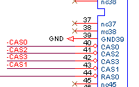
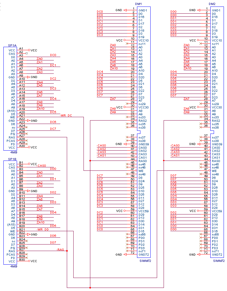
Here is the "adapter" schematic.
This shows how the 2 each 72-pin simms were converted to a dual 30-pin
simm footprint.
Mentally you need to connect all similar "net names" on the sheet,
even if they aren't directly connected by "wires".
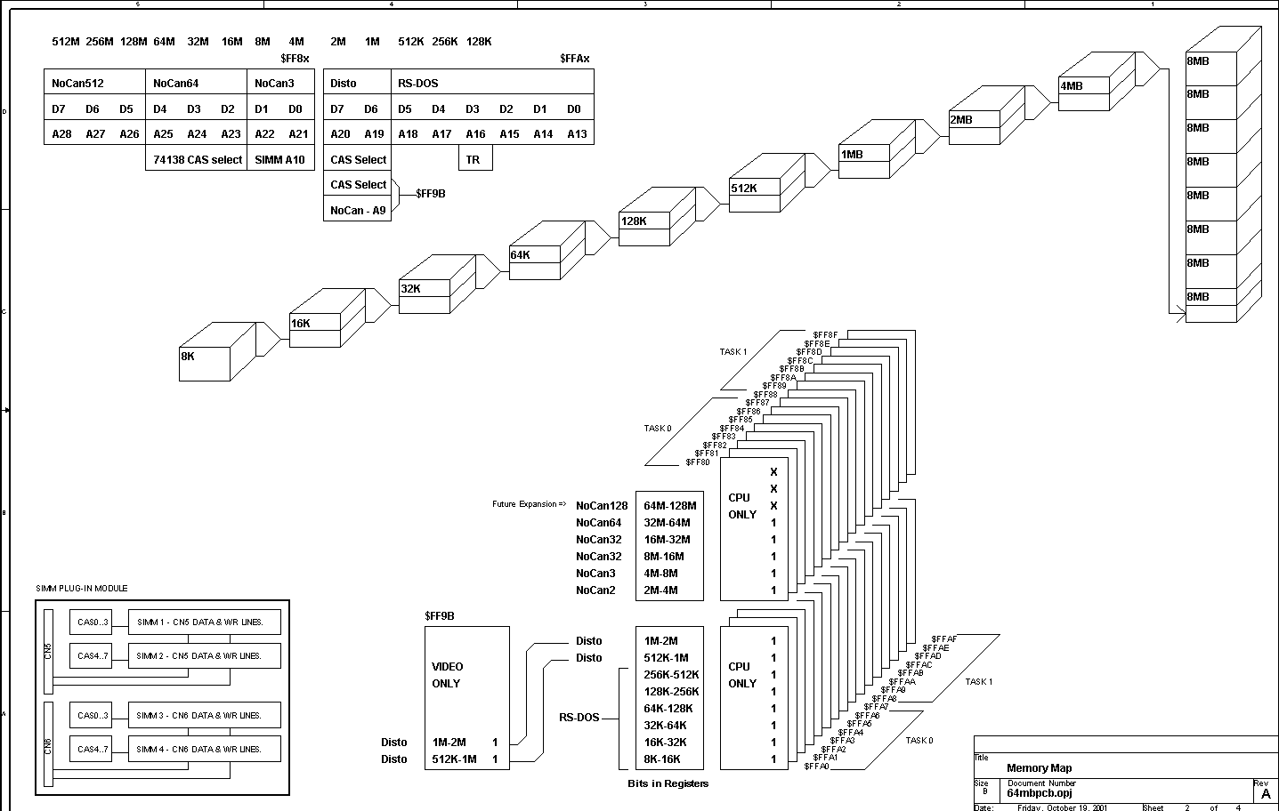
Here is the memory map. It is a really big GIF image 1437 x 912
pixels. It shows how the memory is organized.
If you suspect or find any errors, holler back.
Using only the $FF8X bits allows a user to page through memory in 32
pages (64MB) of 2MB each page, or 16 pages (32MB) of 2MB each page. So,
for a 32MB upgrade, users could have as many as 16 pages of 2MB available
in a single $FFAX + $FF8X page. For instance, this gives 8192 pages
of $4000-$6000.
Address bits for reaching into any block of the 32/64MB uses the bits
as follows: $FFAX + $FF8X. For each $FFAX page the corresponding
$FF8X page extends the addressing by 5 more bits. So now there are
8 + 5 bits for each and every $FFAX + $FF8X page.
Back to Top.
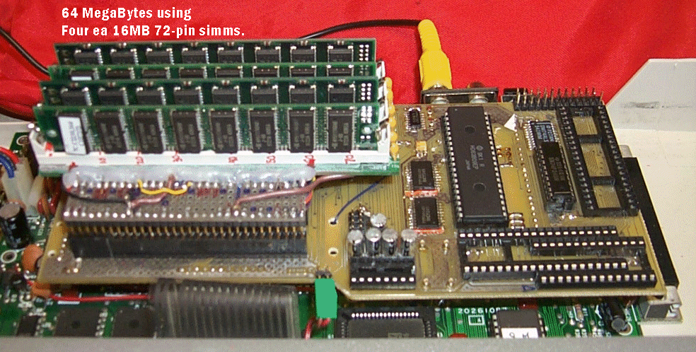
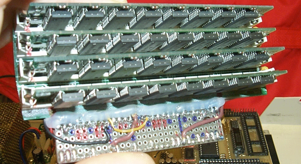
Sorry for the pix quality and focus. In my haste to get them out, they
are kinda fuzzy.
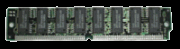
OK. Here's a pix of the whole 64MB. Click on the small pix to get larger
ones.
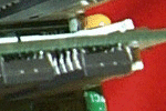
It shows a NoCan3B modified to accept an simm adapter.
This simm adapter plugs into what used to be a dual-angled 30-pin simm
socket, converted to dual-sipp style.
Unused pins (read "cut free") bring in the 7 more -CAS signals.
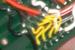
The green header, at the bottom edge of the board having 2 wires, brings
in HSYNC and VSYNC for the CBR refresh.
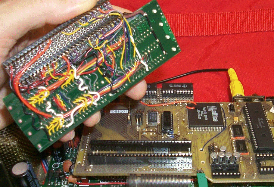
Here's a shot of the bottom side of the "adapter". It has been cut
out from an old unused PC motherboard. Hey, why not!
Some heavy +5 and GND wires along with a strip of hot glue holds the
holey board and this piece of motherboard together.
Not quite in focus are the square pins in a dual row, mounted on the
holey board, that plug into the sipp connectors on the NoCan board.
The two sram's, seen at the back on another piece of holey board, is
the 16x8 sram at $FF8X.
The DAT sram for the original 2MB stuff is seen just to the left of
the Lattice CPLD chip, dip16-74F189.
The SMD chip to the left of that 74F189, is a delay line for the mux,
controlling the RAS/CAS address line switching.
SMD chips to the left of the CPU are address line buffers. What can't
be seen is the SMD R/W buffer just to the right of the CPU.
Oh yes, all SMD chips are hand-soldered, too.
Here's the top view of that "adapter". Not much to see. Just shows
that it was indeed cut from a PC motherboard.
This page updated: 2006/03/02 (yyyy/mm/dd)
Back to Top.