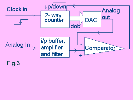
The block diagram for the tracking A- to- D converter is in figure III. The power supply and connections are implied. Neither are connections within a block shown: It is assumed that all IC's have been set up to function properly, that is, enabling inputs connected to the appropriate supply rail and so on.

Substitution of a successive- approximation register for the bidirectional counter will greatly reduce conversion time. Starting with the MSB, each bit is tentatively switched on, but will only stay high if the DAC output of the count accumulated so far does not exceed the input signal level. A start- of- conversion (SOC) signal (a short pulse) must be supplied to clear all bits at the beginning and initiate conversion. An output end- of- conversion (EOC) signal will indicate that the value accumulated is valid. This configuration can provide in excess of 100,000 8- bit conversions per second.
Specifically, the following modifications to figure 3 are required : The counter must have a decoded ouput, that is, each output must pulse sequencially high. A 'Reset' and a 'count inhibit' input is also necessary, while the up/ down' facility is no longer required. The start convertion signal connects to the reset input, while the nth output supplies the count inhibit input- this is also the EOC signal ( n counter outputs, being numbered o(0) to o(n-1), o(0) being the least significant output, correspond to n conversion bits.) Set- reset latches must also be interposed between the sequential counter and the DAC, one for each conversion bit. They will be reset by the SOC signal or by an AND gate fed from the appropriate counter output, the compliment of the comparator output and a slightly advanced version of the clock. Each of their set inputs is connected to another AND gate, driven by the respective counter output bit again, plus a sightly delayed copy of the clock. This is to allow the maximum time for the DAC to settle, without corrupting the remaining conversion bits, because of counter switching.
At video rates, a flash converter can be employed. It comprises a bank of comparators whose one set of inputs is connected to the analogue signal , usually via a sample- and- hold block. The second set of inputs is connected to a resistor chain; the top one is connected to a reference voltage, while the lowest is connected to ground. They may be made variable to allow for contrast and brightness conditioning, respectively. The intermediate resistors need not all have the same value, in order to provide gamma correction. The size of the circuit doubles for each additional conversion bit. If a 'thermometer- type' output will not do, the outputs of the comparators must be connected to a priority encoder chip.
Digital- to- Analogue Converters (DACs) usually come in two
kinds: Ladder type converters provide a current (or voltage)
proportional to the input value. Pulse types, on the
other hand, switch on a constant- current source for an amount of
time proportional to the input digital count, this is, they
modulate the mark- to- space ratio of a constant sequency
rectangular wave, and integrate the resulting waveform. It is
also possible to obtain increased resolution from a converter
having a given number of bits, by using oversampling, but only at
the expense of reduced (maximum) effective throughput.

Fig. 3b: A nice tree to obtain on your oscilloscope using a ramp wave and a successive approximation converter.
Ā