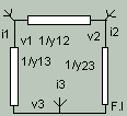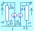
The (floating) admittance (inverse impedence) matrix of a circuit is best illustrated by an example: Figure I is a simple resistive network. To avoid complication, in this particular example, the nodes are arbitrarily numbered and node 0 is left floating (unconnected.) However, this in general will not be the case. Because charge is neither created nor consumed inside a node, the total current into any node is zero. Nevertheless, it is still useful to write down an expression for them. If the currents (rather than the voltages) are the dependent variables, and assuming linearity:
i1 = (v1-v2)y12 + (v1-v3)y13
i2 = (v2-v1)y21 + (v2-v3)y23
i3 = (v3-v1)y31 + (v3-v2)y32
or, rearranging, i = yv

| [i1] | Ā | Ā | [y12+y13 | -y12 | -y13] | Ā | [v1] | Ā |
| [i2] | = | Ā | [-y21 | y21+ y23 | -y23] | x | [v2] | Ā |
| [i3] | Ā | Ā | [-y31 | -y32 | y31 + y32] | Ā | [v3] | Ā |
Now eliminate v3 from all higher equations by the substitution v3 = ( v1y31 + v2y32 ) / (y31 + y32 ). (If more nodes had been present, the additional voltages would have been eliminated iteratively.) Hence, the circuit has been reduced to a two-port network, figure II. If nodes 0, 1 and 2 are always the input, output and earth nodes respectively, it can be shown that:

i0 = y00v0 + y01v1
i1 = y10v0 + y11v1
where ys is the source admittance, yL is the load admittance and Dy = y00y11 - y10y01
The admittance matrix of any linear circuit can be formed by inspection:
The matrix for a transistor is given below. For low frequency work, yre and yoe are usually ignored. yfe is Ie (mA) / (25 mV) approximately, so if (for example) Ie =1 mA, yfe is 1 / (25 Ohms), while yie is yfe / hfe ; therefore if, in addition, hfe = 300 yie = 1 / (300.25 Ohms) = 1 / (7500 Ohms). However, a good design should not depend on the exact value of hfe.
| Ā | B | C | E |
| B | yie | yre | -yie-yre |
| C | yfe | yoe | -yfe-yoe |
| E | -yie-yfe | -yre-yoe | s |
s being yie + yfe + yre + yoe
Notes:
FOR x% = n% TO 3 STEP -1:
a=yr(x%,x%)^2 +yi(x%,x%)^2:
FOR p% = 0 TO x%-1:
FOR q%=0 TO x%-1:
b=yr(p%,x%)*yr(x%,q%)-yi(p%,x%)*yi(x%,q%):
c=yr(x%,q%)*yi(p%,x%)+yr(p%,x%)*yi(x%,q%):
yr(p%,q%) = yr(p%,q%)-(b*yr(x%,x%)+c*yi(x%,x%))/a:
yi(p%,q%)=yi(p%,q%)-(c*yr(x%,x%)-b*yi(x%,x%))/a:
NEXT q%, p%, x%
 The load impedance is negligibly high, in comparison, and the nominal value of the corner frequency, ft is just under 160 MHz. The wire is modelled by a combination of lumped elements (whose number is variable), fig 2b. It does not look productive to use more than about 10 elements. The following graph shows the input impedence, zi, at 160 MHz, in modulus and argument form, against the number of elements used: 1 through 35 (the horizontal axis is logarithmic.)
 Did you want to check calculations, or a subroutine, of your own? Using one element, at 160 Mhz, the voltage gain in deciBels is (20logAv) or -3.04 dB's and the phase angle is -46o (negative, since the current leads the voltage.) The input impedence is 141 Ohms at -44o (capacitive) and the output impedance is 70 Ohms/ -45o. For the sake of those calculations, the source impedance is negligibly low.
Reference: Wireless World magazine (British) Volume 86,
February issue, p.39