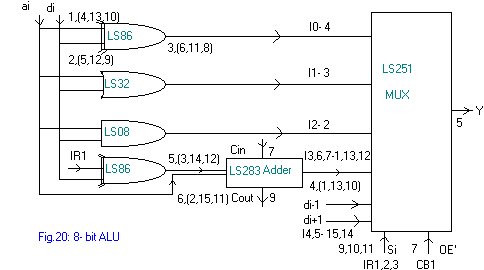
Power Supply Connections: ICs LS86, 08, 32: Vcc~14 Gnd~7; LS 283, 251: Vcc~16 Gnd~8;
The And, Or, Xor and adder chips are 4- bit wide, so two of each are required: Also 8 multiplexers will be needed. Although offering different functions, the Or, Xor and And chips otherwise have an identical pinout.
The schematic is shown for one bit only- numbers in parentheses show the pin allocations for more significant bits.
The adder is driven from a Xor gate, so that it can provide subtractions, as well: The carry output of the low order adder (pin 9) must be connected to the carry input of the high order adder (pin 7). The overall carry (or 'borrow') output is of course taken from the high order chip- the low order LS283 carry input is driven by the carry flag. The carry is cleared by using a CLC instruction prior to adding a single byte (or the low order byte of an integer comprising several bytes.)
For subtraction, the data inputs are inverted, and the carry is set (for a single byte operation, or for the low order byte of a multi- byte sequence.) The Xor gate that complements the inputs is driven by bit 1 of the instruction register. There is no difference between the comparison and subtraction operations, other than the fact that for comparison, the ALU output is not recorded, only the status register is affected.
For a right rotation operation, each bit is replaced by the bit having an immediately higher binary weight, while the carry output is supplied to the MSB, and the LSB is driven to the carry input multiplexer at the status register section. For a left rotation operation, each bit is replaced by the bit having a directly lower weight, while the carry output is supplied to the LSB, and the MSB is eventually driven to the carry input. To effect a right/ left shift, the carry must be cleared beforehand, using a CLC instruction. (This is also necessary before multiplying the low order byte/ dividing the high order byte of an unsigned integer by two.)
The multiplexer select inputs are driven from bits 1, 2 and 3 of the instruction register, and the output enable signal is provided by a decoder in the control section. The multiplexer inputs (0-7) are allocated so as to simplify the task of the carry input selector; (the carry must also be loaded from memory when the flags are.)
The temporary data register (TDR) provides one set of inputs to the ALU, while the second set is provided by the Accumulator; there is an extra buffer between the Accumulator outputs and the data bus- it is enabled when the Accumulator contents must be stored in memory. The ALU output is placed on the data bus, and from there latched into the Accumulator. There is an apparent alternative: Using a multiplexer at the Accumulator inputs to select between the ALU outputs and data bus, and feeding the ALU from the data bus, after placing the Accumulator outputs there. This, however would have resulted in a slower microcontroller.
The ALU is in the tradition of old microprocessors, where the Accumulator both provides one of the operands and records the result: In modern style processors, any register can provide either of the operands and store the outcome of functions. However, this requires additional multiplexers at the ALU inputs, as well as more bits allocated in the instruction byte, in order to drive them, and activate the appropriate latch input of the register which receives the result.
Most of these functions can be provided by the 74LS281 or equivalent 4- bit ALU chip. Extension to 16 or more bits is not entirely straightforward, because of the need still to cater for operations between shorter wordlengths.
When the next microcontroller section appears, it will present the register board.
- Today's Random Fractal
- Fractal variations!
- Site Index (Frames Version)
- Site menu (Non- Frames Version)
- Twin- T Filter
- High- Frequency Oscillators
- Walsh Transforms