Useful Circuits
Maximum Current Limiter
The circuit below shows how to
construct a circuit that can limit the current delivered from the power supply
to the load R3. Note that R2, R4, and R5 are used as a voltage divider to
establish the BIAS point of Q2 transistor when Q1 is OFF. R5 must be small
enough to allow sufficient current to flow through the load and through Q1
collector to emitter junction. You may start in your design with 100 ohms
resistor for R5. Zener diodes D1 and D2 are
selectable such that they will match the output voltage requirements. When too much current flows in Q1 or the load the base of Q2 starts
to rise and thus renduring more current flow through
Q2. This will cause the base voltage of Q1 to drop and thus the current
through Q1 dropes as well. This acts as a feedback to
control current flow through Q1 depending on the setting of R2, R4, R5, D1, and
D2. To gain flexibility in selecting the required current through the load R3
you may use variable resistors or potentio meters in
place of R1 and R4. If your output voltage requirement is low then you may give-up
D1 and D2 from your circuit. Remember that current sources are different from
voltage sources such as current sources have fixed output current but may have variable
voltage at output.

I successfully used the above
circuit to control the current delivered to my amplifier used in one of the
security systems I designed. Note also the Q1 current rating must be chosen
accordingly depending on your application.
Feedback
trick with T- Resistors Network
At a times we need use the Op Amp to produce high
gain while keeping the input resistor high. This configuration is desired in
designs such as in Integrator:
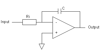
or Programmable Gain Amplifier (PGA) with
DAC used as a variable resistor at the input:
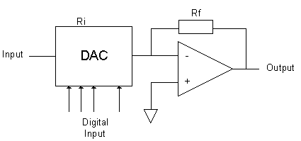
The input resistor is by nature
large and is assumed to be impossible to replace with smaller one. If the
feedback resistor (Rf) is
too large, to accomplish high closed loop gain, the circuit will drift the
output and circuit may become unstable. In order to accommodate a feedback
resistor in this design that keeps the gain in action a trick is used in which
the feedback resistor is replaced with smaller common value resistors (in a
T-network) while maintaining relatively large input resistor and delivering
decent gain:
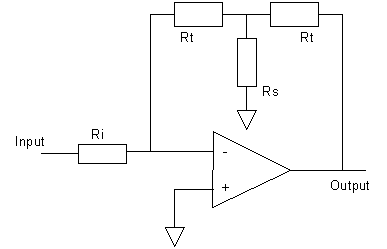
The input resistor remains
relatively high so when it is in action (such as connected to a photodiode or
it can't be smaller) minimal current flow into Ri while the T-network resistor in the feedback path
behaves as a large value resistor. For example, to produce an overall gain of
-100 use an input resistor Ri
of 100K, Rt of 100K, and Rs
of 1 K. In this example the T network behaves like a single 10M resistor. The
current drift will then be almost gone and circuit becomes more stable.
Zero
Crossing Circuit
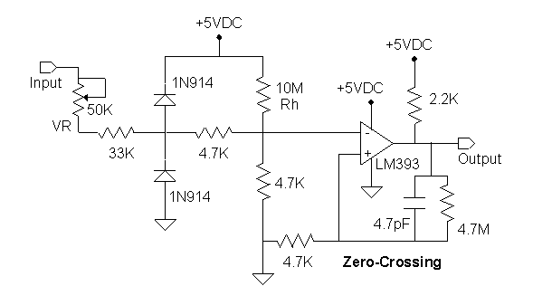
The following circuit will provide an
output pulse or square wave when an AC signal at the Input crosses the zero volt. VR adjusts the input AC voltage up to 120 VAC. Rh will set the trigger point around the ground. Insure to
use a comparator (such as LM393) that can accept 0 at inputs for single supply
operation.
Second
Order active Low Pass Filter
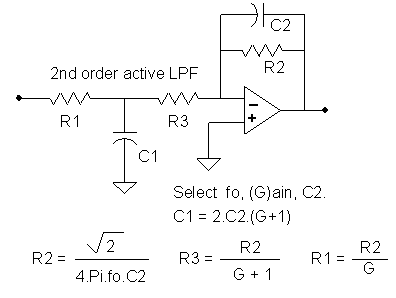
The following Low Pass Filter
(LPF) circuit is a very useful circuit, it is used in
so many modern circuits. Cut off frequency (3-dB or half power) is programmable
as per simple equations below. It can be cascaded with another 2nd LPF circuit
to generate 4th order LPF, or with 1st order LPF to
generate 3rd order LPF. Insure that the frequency response of the Op
Amp you are using can span the frequency of interest you are using. Also do not
expect too much gain when dealing with Active LPF. You may use a 0.1 uF cap at the input/output of this circuit to prevent any
DC component from leaking into the Op Amp inverting input.
Second
Order active High Pass Filter
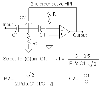
This circuit can be used to
filter out Low Frequencies and pass the high frequencies. Corner frequency
(half power or -3 dB) is programmable via few components as per equations
below. It can be cascaded with another similar High Pass Filter (HPF) to form 4th
order High Pass Filter, For first order filter the
roll off will be 20 dB per decade, and for 2nd order will be 40 dB per decade,
oh did you say that for 4th order the roll off will be 80 dB per
decade? You are correct. It also can be cascaded with the LPF above to form a
Band Pass Filter (BPF). Remember that corner frequency alignment (fo) of LPF and HPF to form Band
Pass Filter will determine the bandwidth of the resulting BPF. For High Quality
Factor (Q) the fo for both
filters should be same, the roll off of both filters will convolute on one
another forming response skirt following the roll off for both filters. For
wider band width the corner frequencies for both filters should be designed to
position on the frequency axis far from one another depending on your
application and how much band width you desire. It is you who decide the band
width. Insure that your Op Amp has the Gain Bandwidth Product your circuit
requires. Also do not expect high gain when designing with filters. The gain
you selected shouldn't drive the output at anytime to higher voltage than the
supply assuming that you are using rail-to-rail Op Amp.
Determining
the required order of the filter
Down Load my easy to use calculator to find the
order of the LPF filter you are designing. You may cascade, in series, several
first-order, second order, or higher order filters to achieve the required
attenuation at the required operating frequency. When cascading filters make
sure to line up all -3 dB and MAX attenuation frequencies properly, this is
based on the fact that transfer function of different circuits will convolute
on one another and the final frequency response is unlike the individual
frequency response of the individual filter. Your circuit will not work
properly if the dB per Decade is not selected properly. Email me with
confidence if you have any question or design requirement/s.
Peak
Detector
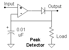
This circuit is a
self-explanatory, it outputs the MAX input (Peak Detect) that shows up on the
input.
Logic
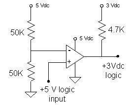
Level Translator
This circuit translates 5 volts
logic level to 3 volts logic level. Choose comparator that has rail-to-rail I/O
and open drain output or complementary output configuration. Also chose it with
hysteresis feature.
Do you
have any design problem? Feel free to email me at fifaham@yahoo.com with any of your design needs.
![]()
By Engineer: Firas Faham