Simple Transistor Driver Circuit
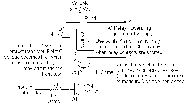
This is very simple transistor driver circuit used to drive any load (connected to the relay X and Y points.) This load could be a motor, light bulb, solenoid, water pump, or any other power device. Make sure the load connected to the relay X and Y contacts is compatible in power with the power rating of the X and Y relay contacts MAX power ratings. See relay specs for info Before you buy it.

After you build this
Transistor Driver circuit above manually adjust potentiometer (or variable resistor) VR1 to a value that will turn ON the relay and shorts contact points X and Y. If you don't hear the relay clicking (may have soft contacts or noisy environment) use the ohm meter to test for points X and Y short circuit when transistor is ON.When the Input connected to R1 (Input to control) is high transistor Q1 turns ON and puts the relay coil of RLY1 in the transistor collector to emitter current path turning ON the relay and shorting the relay contacts points X and Y. When the Input goes low the transistor turns OFF and relay contacts X and Y opens disabling the load. Notice that we cannot let the signal at the Input control the relay contacts X and Y directly because the high voltage high current load at points X and Y may damage the circuit connected to the Input.
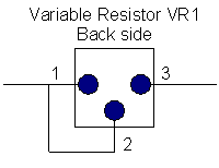
Variable resistors come in different tastes, they may be rounded, squared, rectangular, or other. Here is a basic diagram for connecting the VR1 potentiometer to the circuit. Notice how pins 1, 2, and 3 connect to the circuit above. See the specs for connecting the VR1 properly to the circuit above. Also notice that pin 2 in the diagram below may have different pin number on the data sheet. In the diagram below pin 1 and 3 have fixed resistance value, pin 2 only will vary its value relative to pins 1 and 3. If pins 1 and 2 value becomes smaller then pins 3 and 2 reading value will get larger and vise versa.

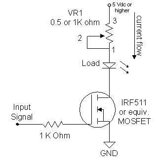
Another variation of the transistor driver is the power MOSFET transistor driver shown below. MOSFETS cost a bit more (depending on power handling capability and speed.) They can handle much more power than their cousin BJT transistor above. IGBT is another variation of the transistors but again cost more, they are the born baby of BJT and MOSFET transistors. The load below is shown as an
LED, replace it with any real load that is compatible with the power handling capability of the Drain to Source current rating of the MOSFET you are using. Use any VR1 max value of 500 to 1000 ohms to limit the current going into the load. The MOSFET used below is part number IRF511.
The MOSFET is a voltage controlled device while the BJT transistor 2N2222 above is current controlled device. This results in very little or zero current needed to turn ON the MOSFET via its Gate but the BJT needs some current to turn it ON. When the transistor turns ON current flows from collector to emitter in the NPN BJT or Drain to Source in the MOSFET (N Channel.) BJTs and MOSFETs come in different flavors that will be covered later.

Remember to place reversed
diode whenever you have an inductive load powering from the transistor driver. This is the case when high voltage is induced across the switch transistor because of sudden stop of current. Use any signal source to control any load as shown above. An example is controlling a water pump (high power load) from the output of the RC (remote controlled) small racing car you bought from the garage sale or from the output of your Microcontroller. The Microcontroller may not be able to power up power devices so the driver is then needed. You may get the relay from junk old equipment or you can buy it from Radio Shack store closest toy you. For different signal values manipulate VR1 above for best response. As the supply voltage (battery) ages you may need to re-adjust VR1 for optimum response. For better results use fixed power supply from the AC to DC adapter. Also see part number LM7805 or LM7809.Have fun…
![]()
Engineer: Firas Faham