Small Signal Amplifier Design
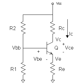
If the amplifier must operate reliably and maintain decent gain, noise figure, and stability over large temperature extremes a DC bias network must be carefully designed. The DC operating point must be stable under all specified conditions otherwise the gain characteristics will suffer and specially when dealing with higher frequencies. Transistor parameters that influence the transistor DC operation over temperature change and need to stabilize are D b and D Vbe. The b of a Silicon BJT transistor increases with temperature at a rate of approximately 0.5% per 1 °C causing the total transistor set gain to divert from the intended value. Also the transistor base to emitter voltage Vbe decreases at a rate of about 2.5 mV/° C from normal room temperature value of 0.7 Volt. Changes in Vbe parameter due to wide temperature change may cause change in the collector to emitter current leading to undesired changes in the collector to emitter voltage. The following amplifier design enables a reliable and stable DC biasing and operating requirements:

For a good design practice the Rb parallel equivalent of R1 and R2 should satisfy the following:
Rb / Re < 10
Since Vbe changes with temperature and most applications operate over temperature variation of +/-50 °C this leads that for Vcc of up to 20 Vdc an emitter voltage selection of 2 to 4 volts (depending on Vcc) will provide around +/-5% in Ic variation due to D Vbe.
Here are the design steps:
A. Assume Ic of 10 mA (from data sheet) and depending on Rc or load power requirement.
Vc = 10 Vdc (assume half Vcc for maximum voltage swing)
Vcc = 20 Vdc (operating DC supply) and can change
b = 50 (
obtain from data sheet of transistor)
B. For stability assume Ve = 2.5 Vdc, see above.
C. Assume Ic = Ie since b is >> 1
D. Re = Ve / Ie = 2.5 / 10 mA = 250 ohms.
E. Rc = (Vcc - Vc) / Ic = (20 - 10) / 10 mA = 1 K ohms
F. Ib = Ic / b = 10 mA / 50 = 0.2 mA
G. Vbb = Ve + Vbe = 2.5 + 0.7 = 3.2 Vdc
H. To insure the transistor is properly biased via the base choose Ibb to be larger than Ib, such as Ibb = 1.5 mA
I. R1 = Vbb / Ibb = 3.2 / 1.5 mA = 2133 Ohms
J. R2 = (Vcc - Vbb) / (Ibb + Ib) = (20 - 3.2) / (1.7 mA) = 9882 Ohms
So now you solved for Rc, Re, R1, and R2. You may select Ibb to be higher and still get decent results. Remember that higher values of Ibb means guaranteed biasing for Q and lower values of Ibb means more chances to noise interference. You may need to strike a balance between large and small Ibb values depending on the power supply available and its age requirements and Ib that is determined from Ic. Keep in mind the formula above: Rb / Re < 10. In mass production this is the best amplifier configuration for your design requiring no calibration or fine-tuning for biasing after production so try to keep your Ibb relatively high enough to avoid noise interference and proper biasing but low enough to avoid battery drainage. Also different Vcc supplies will lead to different Rc values. Note that Re was determined by Ve and Ie while Rc was determined by Vcc, Vc, and Ic. Depending on your design you may need to tweak your Vc to levels acceptable by the input signal level at Vbb and b factor of your transistor. Insure that the maximum output at Vc will not exceed your power supply Vcc to avoid unnecessary distortion if swing goes beyond MAX or MIN swing. So adjust your input signal level accordingly if needed and design parameters accordingly. If the output levels are low then follow this circuit with a cascaded and similar amplifier. You may need to couple these two stages via a capacitor, see Coupling section of my other web pages.
When coupling stages you are connecting the output of the first stage to the input of the second stage. Any DC leakage from the output of first stage may disturb the Biasing of the next stage thus changing it's operating point and nulls amplification, so play it safe. The AC coupling capacitor will block the DC from the first stage and thus amplifying only the AC signal components passing from stage 1 to stage 2. In this case the Coupling capacitor may act as a High Pass Filter (passing relatively high frequencies and rejecting lower frequencies) so make sure that the coupling capacitor you are using added to the biasing resistors of the next stage can collectively and actually pass the signal frequencies you are interested in, because capacitors and resistors in this configuration may act as a High Pass Filter.
![]()
By Engineer: Firas Faham